
No.8 "How small the thermoelectric module could be?"
The last story was "How thin the thermoelectric module could be?" This time, the story goes the other aspect; thinning and miniaturization. You may have thought once at least that what could happen when you make the cross section of the element of the thermoelectric module smaller and smaller, e.g. several tens of microns as illustrated in Fig.1, without changing the heat pumping capacity: Imax and number of element couples. What the performance of the miniaturized module could be?
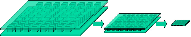
Fig.1 Shrinking a TEC without changing element Imax and couples
Note: Dimensions of parts are decided by the conditions below.
• EElectrode length=Element section×2.75
• EElectrode width= Element section×1.2
• EElectrode thickness=Electrode width×0.5
• EElement pitch=Element section×1.65
• ECeramics thickness(mm)=0.5-0.1(practical value)
As we keep the Imax and element couples unchanged, miniaturization naturally suggests a detrimental effect on maximum temperature difference, ΔTmax, from increasing electrical resistance of copper electrode, solder and NiP plating(see Fig.2), and also from increasing thermal resistance of copper electrode, solder and NiP plating except thermoelectric element(see Fig.2).
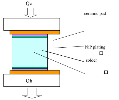
Fig.2 Material configuration of a heat flow unit of the thermoelectric module
In calculation of ΔTmax, the conditions were set to those shown in Fig.1 and Table 1. To get a guideline to decide the thickness of electrode, a simulation shown in Fig.3 has been made.
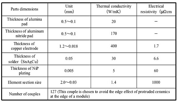
Table 1 Materials constants used in calculation
Fig.3 Effect of electrical resistivity on ΔTmax(Current density of electrode=constant)
The larger the element section size, the less current density of the electrode should be taken.
From Fig.3, when element section is changed with constant current density of electrode, you can find a peak section size at which maximum ΔTmax value is achieved. It shows that ΔTmax deteriorations do not depend on the current density if the section is below 0.2mm, however if the element section exceeds 0.2mm, ΔTmax deteriorations become larger with the increasing section size of the element. This is because, even if current density is kept constant, the length of electrode gets longer with the increase of element section. So, you have to be aware to reduce current density in accordance with the section size extension. In this article, for the elements having larger than 0.3mm section, thickness of the electrode is arranged not to pose ΔTmax deterioration from this cause.
Practically used element section and electrode thickness are described in Table 2. Smaller sections, corresponding to fiber-optic telecom use, have thin electrode and high current density because of low profile requirement to these products.
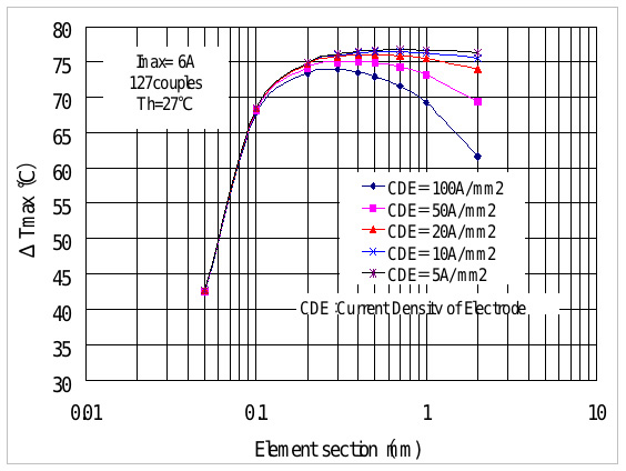
Table 2 Electrode current density of practical thermoelectric module
ΔTmax deterioration from electrical resistances of electrode, solder and NiP plating becomes very large when element section gets very small.
ΔTmax deterioration from electrical resistances of electrode, solder and NiP plating becomes very large when element section gets very small.
As the loss in ΔTmax includes not only of electrical resistances but of thermal resistances, the minimum section size would naturally be larger than those can be seen in Fig.3.
Fig.4 Effect of element section on ΔTmax(Electrical resistance)
If you choose alumina ceramic pad, the element section cannot be so small.
Fig.5 shows the detrimental effects of electrical resistance and thermal resistance on ΔTmax in the case of alumina ceramic pad. With the increasing Imax, harmful effect of electrical resistance plus thermal resistance on ΔTmax gets larger. Using alumina, the minimum section to obtain ΔTmax=70°C is still 0.7mm(Imax=6A). Even if you reduce Imax to 3A or 1A, it can only be shrunk to 0.5mm or 0.23mm.
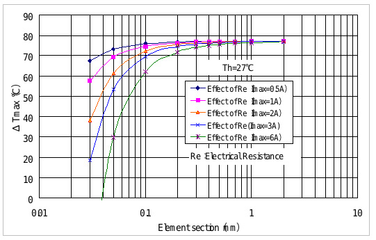
Fig.5 Effect of element section on ΔTmax (Electrical resistance plus thermal resistance)
If you choose aluminum nitride ceramic pad, you can get much less size of element section.
Fig.6 shows the case using aluminum nitride. The minimum section to obtain ΔTmax=70°C is 0.4mm(Imax=6A). If you reduce Imax to 3A or 1A, it reaches to 0.26mm or 0.15mm. So, it sounds you can get much less element section if you choose aluminum nitride.
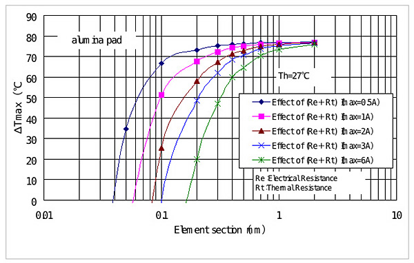
Fig.6 Effect of element section on ΔTmax (Electrical resistance plus thermal resistance)
Table 3 shows the minimum element section sizes to get ΔTmax=70°C for different ceramicses and different Imaxes.
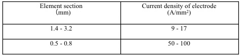
Table 3 Minimum element section to get ΔTmax=70°C(Unit:mm)
The detrimental effect of thermal resistance on ΔTmax is much larger than that of electrical resistance.
three curves correspond to electrical resistance effect, thermal resistance effect of alumina and thermal resistance effect of aluminum nitride respectively.
As you have already noticed from the explanations so far, thermal resistance effect of ceramic pad is much larger than that of electrical resistance.
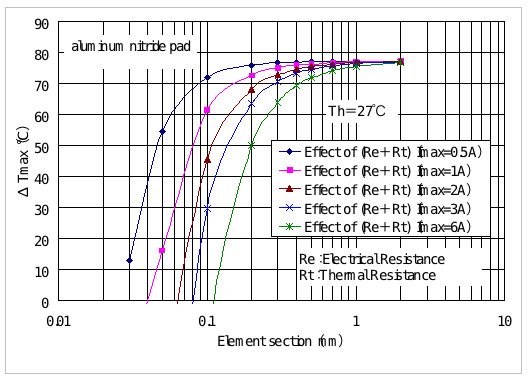
Fig.7 Effect of element height on ΔTmax (Separated effect of Re and Rt)
If we want to make element section smaller and smaller without deterioration of ΔTmax, we really need such materials as diamond and carbon nano-tube!
The conclusion may be that if we want to shrink the element section of the present practical thermoelectric module by one tenth or smaller, it seems that we have to have an insulation pad material with very small thermal resistivity like diamond and also an electrode material with very small electrical resistivity like a kind of carbon nano-tube.
Written by Yasutada Kibayashi